Difference between revisions of "Full adder"
From Fixme.ch
| Line 15: | Line 15: | ||
From this chip, we would like to make a adder. It is one of the basic component of everyCPU. It's use is to have two bits. They represent a state either 1 or 0. We will add them with the following scheme : | From this chip, we would like to make a adder. It is one of the basic component of everyCPU. It's use is to have two bits. They represent a state either 1 or 0. We will add them with the following scheme : | ||
| + | <pre> | ||
1 + 1 = 10 | 1 + 1 = 10 | ||
1 + 0 = 01 | 1 + 0 = 01 | ||
| Line 23: | Line 24: | ||
^ this bit is the most significant bit. We call it C1 later on. | ^ this bit is the most significant bit. We call it C1 later on. | ||
^ this bit is the least significant bit. We call it C0 later on. | ^ this bit is the least significant bit. We call it C0 later on. | ||
| − | + | <\pre> | |
Just follow the | Just follow the | ||
Revision as of 23:42, 14 May 2012
Contents
Goal
- First step into logic
Level
- Knowing how to use a breadboard
Component
- Only one logic gate array.
How to
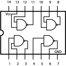
The logic circuit of the chip is as followed :
From this chip, we would like to make a adder. It is one of the basic component of everyCPU. It's use is to have two bits. They represent a state either 1 or 0. We will add them with the following scheme :
1 + 1 = 10
1 + 0 = 01
0 + 1 = 01
0 + 0 = 00
^ this bit is the first bit we add, we will call it A later on.
    ^ this bit is the second bit we add, we will call it B later on.
        ^ this bit is the most significant bit. We call it C1 later on.
         ^ this bit is the least significant bit. We call it C0 later on.
<\pre>
Just follow the

[[File:Halfadder.gif]]

== What is happening there ? ==
